From Schematic to Stripboard
September 2012 © http://tagboardeffects.blogspot.com
Updated 23rd September 2012
A lot of people have asked me if I could do a guide to show the methods I use to convert a schematic to a layout so I thought it was about time I came up with one. I’ve always been of the opinion that the more the merrier when it comes to layouts. The more people that are doing them, the less I may have to do myself and I do have a social life that I’d like to keep! :o)
There are a few people out there who have produced fantastic layouts, going back a few years we had Torchy who was the first person to get me into vero layouts, and shortscalemike really inspired me when he was coming up with layouts for popular effects. But I have major OCD with pedal building and only started doing these layouts in the first place because I want everything to be perfect for me. So my criteria for the perfect layout would be:
1) No standing axial components. EVER! I hate them with a passion. Some people like timmy on here can make standing components look elegant by the effort he puts into the build, but it never turned out that way for me, and most of the time I see them I think they look awkward and haphazard. It’s not just the look that makes me want to avoid them though, or the fact they look susceptible to being knocked and bent. I love to have a board in a vice, stuff all the resistors in one go and then lock them down, turn the board over and solder them all in, and standing components stop that from happening. I’m sure plenty of people disagree with my philosophy here and I’ve been criticised in the past because my layouts were slightly larger than someone elses (although that isn’t always true, there are a lot of layouts on here where mine are the most compact of the ones available), but my OCD has given everyone almost 300 verified layouts to choose from thanks to some wonderful people on here, so those complaining can’t moan too much. If they prefer to save a couple of rows in some effects where I have sacrificed compactness for form, then I won’t be upset if they use someone elses, and it’s not like I can offer them a refund.
With the above in mind, I’m not interested in the slightest in reducing a 17 x 9 vero down to 15 x 7. They’ll both easily fit in my most commonly used box and so why make something compact that doesn’t need to be made compact? I’d prefer the extra board space to make it easier to build, fault-find and/or mod.
2) Despite point 1, depending on the number of pots and switches I like to keep the board down to a size that would allow it to fit in the most appropriate box. 4 pots and less I want to make sure it can fit in a 1590B, anything more than that (or when it has switches as well which take up just as much room) then I want to make sure it can fit comfortably in a 1590BB. Virtually all of the layouts on this blog (with the exception of some of the earlier tagboard layouts) will fit in a 1590B. So that means the absolute maximum width is 22 vero columns (tight fit and needs filing down at the sides slightly) but most of the time I will aim for an absolute maximum of 21 columns wide and preferably narrower to allow more of a gap for wires.
3) The number of rows doesn’t bother me as much. If you’re mounting the board on the back of your pots with the components facing upwards then the sockets can limit you, but if you turn the board round and mount it with the components facing downwards as you look in the box then you have much more room, especially if you haven’t left space for a battery. You can easily get 22 rows in a 1590B and even more if you’re careful about the placing of some components to physically avoid offboard sockets. So a Klon may be a struggle (although I bet it could still be done with my layout on here and by a determined builder) but I think everything else around 24 rows should fit in no problem.
There are other things but I don’t want to write ‘War and Peace’ about it, so I’ll leave it with the most important three criteria to me.
———————————-
I didn’t want to choose a small circuit like a Super Hard-on for this because it’s too simple and wouldn’t give me enough of an opportunity to explain why I do certain things. But likewise I didn’t want to choose something too big where people would lose the will to live before we got to the end. So I thought a good example for something like this would be something like the Lovepedal Eternity.
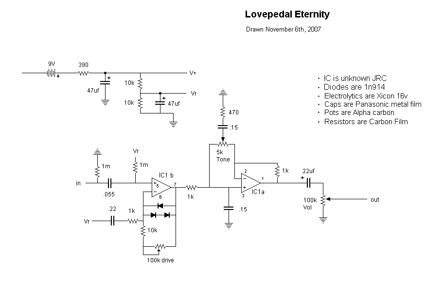
So this is the schematic I’m working from:
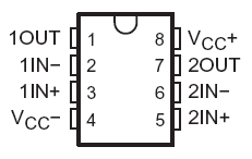
And an overview of the IC pinouts:
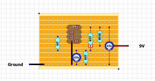
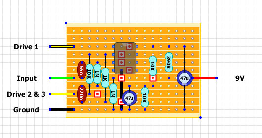
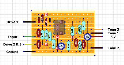
Firstly I look at the schematic and see if I can estimate the final width to determine how many columns and rows I’m going to need. With some effects like the Big Muffs there is a long row of cascading stages and so I know with something like that I’m going to have to do it in two levels to keep it 1590B friendly, left to right at the bottom for the first half of the circuit, and then right to left at the top to finish off the second half. With the Eternity though there are no buffers and the circuit is fairly simple so I know that it will easily fit on a board with 21 columns or less meaning I can do this simply enough on a single level run from left to right. With it being an IC circuit I tend to estimate 11 or 12 rows depending how many additional components I’m going to have to add, so here I have a board starting off at 16 columns by 11 rows to start off with, and place the IC in an appropriate place.
I always use the bottom row as a ground rail so it is easily available to take components to ground from anywhere on the board, and so put a link in from the bottom row up to IC pin 4 to make the required ground connection to the opamp.
Next I put in the components required for the power side of things. There is a 390R resistor in series with the supply and so I put that in up to pin 8 of the IC so make the V+ connection. From V+ there is a 47uF capacitor to ground to filter out noise from the power supply and smooth ripple, I have put in a radial capacitor here but would probably actually use an axial capacitor myself for this because there are much better suited to this sort of span of rows than the radial caps are. There is a 10K resistor from V+ to Vref (half supply voltage), and from there another 10K goes to ground to finish off the voltage divider. In line with my philosophy, I always choose the location of the Vref row so that a resistor can lie flat to V+, and flat to ground. The voltage on that row would now measure 4.5V as required. Another 47uF filter cap to ground from this row and then a link up to IC pin 3 via a 1M resistor and that is the power side of things finished with.
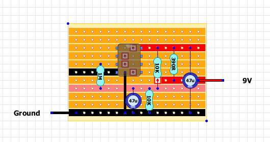
So this shows the supply rows as the layout currently stands, black is ground, red is V+ and pink is the Vref 4.5V row. Incidentally, that ground rail from pin 4 of the IC comes in really handy sometimes if you want to ground components from one of the rows above the IC without having to go all the way down to the bottom row. You’ll see that done on a few of these layouts.
I always start the signal path on the left and finish on the right, then the input and output wires are the correct side of the board when the vero is mounted on the back of the pots in the conventional way with the components facing up. So from the input we have a 1M pulldown resistor to ground and a 55nF cap up to the non-inverting input (pin 3) of the IC (you’ll notice I’ve changed the numbering from the schematic so I’ve swapped pins 1 to 3 around with pins 5 to 7 which allows me to run the circuit from left to right as I prefer. This is a dual opamp and there’s no issue with using the left hand channel first or vice versa). I use Panasonic or polyester box caps most of the time which have a 5mm pitch, so ideally I want a 3 row span from the capacitor. I place the cap accordingly and under the IC I put in the 1M pulldown resistor. I put that in position under the IC basically because it will go there and so not interfere with any components that I need to place on the left side of the board. Putting a cut after the top of the 1M means I have 3 holes further up the same row which I can use later if I need to. Remember that just because the schematic shows the 1M first, it doesn’t mean you have to put it closest to the input wire on the board. This is electricity which moves pretty fast and so you can make the connection anywhere on the row and it will perform its intended function perfectly well.
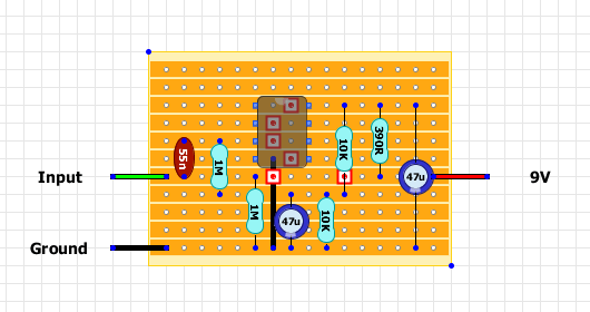
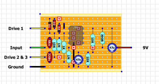
From the inverting input (pin 2) there is a high pass filter to cut some bass before the gain stage so things don’t get flubby. This is a 1K resistor followed by a 220n cap to the Vref row, and because I’m using 5mm pitch caps (and want to stick to a 3 row span where
possible) I need to place the bottom of the 1K resistor 2 rows away
from Vref. So they go in the only place that can meet that criteria as shown, with a cut again put to the right hand side of the series connection so I can use the same row further down for something else.
Next there is a 10K resistor that goes between the inverting input (pin 2) and lugs 2 and 3 on the drive pot, so this goes in an appropriate place with the usual added cut. This resistor sets the minimum gain available from the Drive pot in its far counter clockwise rotation, so if you want more gain in the lowest setting increase it, if you want less gain decrease it. Lug 1 of the pot connects to the output of the first opamp channel (pin 1) and so I can add the connections for the Drive pot.
I now add the asymmetrical clipping diodes. D1 and D2 make a series pair which go in the feedback loop between pins 1 and 2 so those connections are easy enough to make using the top row as the series junction, again with a cut to isolate it from the rest of the row. D3 however needs to go between 1 and 2 on its own which would mean having a standing component. No thank you, so I add a small link between pin 1 and the row above so I can keep the diode lying flat. This gives me an added advantage which I will come to in the next section.
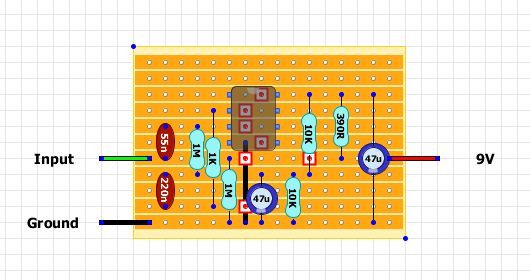
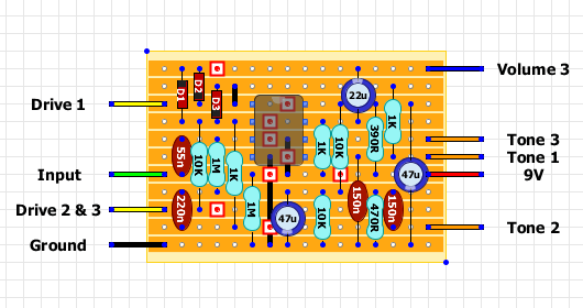
The schematic shows a 1K resistor between the output of the first opamp channel, and the non-inverting input of the second. This causes an issue because they are on opposite sides of the board and so I can’t use a single component to make this connection unless I mount the resistor over the top of the IC. But that little link that I used for D3 has given me exactly what I need, a connection to pin 1 from the right hand side of the board, so I can just take a 1K resistor from the second row down to non-inverting input (pin 5) and that connection is made followed by a 150nF capacitor to ground (again this shows a 5mm pitch Panasonic type cap but they have long leads so there’s no problem spanning multiple rows using them, or you could use an axial cap of some sort if you prefer). When I use links they often have two functions like this which actually goes to make things easier in the long run. The 1K resistor followed by the 150n cap to ground is a passive low pass filter to cut some high end after the gain stage. It starts attenuating at 1061hz, and so all frequencies below that are allowed to pass, frequencies higher are rolled off at 6dB per octave, meaning the signal amplitude is reduced by half every time the frequency doubles.
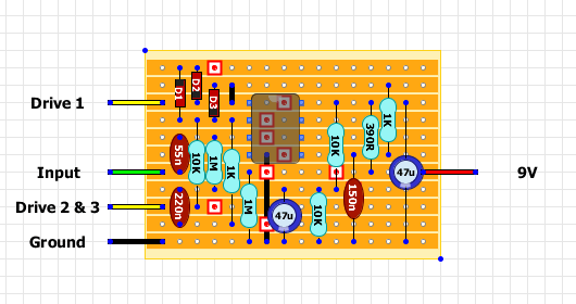
You can see that the outer lugs of the Tone control are connected to the inverting and non-inverting inputs of the right hand channel and so I place those wires in the layout.
Lug 2 of the Tone control connects to a 150nF capacitor and then a 470R resistor to ground, and as I have no need to continue the Vref row, I can place them as shown and put a cut between the top of the 470R and bottom of the 10K (obscured by the 150nF cap between them). The 150n and 470R combination to ground attached to Tone 2 creates a 2.2kHz RC network and rotating the tone pot to the extremes either “attaches” it to the inverting or non-inverting input. When at the non-inverting input (pin 5) frequencies above 2.2kHz are dumped to ground and so some high end is rolled off. When at the inverting input (pin 6) feedback frequencies above 2.2kHz are dumped to ground giving a treble boost by countering the roll off created by the 1K/150n low pass filter at pin 5.
Nearly finished now, you can see that a 1K resistor is required between the right hand channel inverting input and output (pins 6 and 7). Again this would require a standing resistor and so I can make use of those 3 free holes mentioned earlier and put the 1K from 7 with a link up to 6.
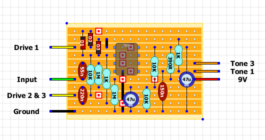
The only thing left is the output capacitor, so I can take that from pin 7 up to the top row making sure the negative leg is to the top, and then add the wire connection for Volume 3 lug to the right hand side of the row.
And that’s your layout finished. Just add any notes required about the components or additional connections, remove any unrequired cuts if you want to (the Drive 2 & 3 cut isn’t needed but I just left it anyway), and you are done.
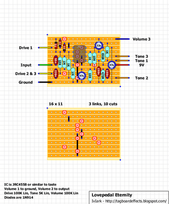
I may add additional layout guides in the future to show other things that haven’t been covered with this layout, such as the Big Muffs or some of the popular JFET effects to show how I tend to deal with transistor circuits. If you have something that you think would be useful to cover in this kind of guide then let me know and I can get a consensus of what people want to see.